
-
High Light
oem rapid pcba
,telecommunications rapid pcba
,1.0oz rapid pcb assembly
-
Product NamePCBA
-
MaterialFR-4,High Tg FR-4, Halogen Free FR-4, Thick Copper FR-4, Aluminium Based, Rogers, Taconic
-
LayersDouble Side ,Multilayer (Customized)
-
Copper Thickness1.0oz 2oz ...... 6oz
-
Min. Line Spacing0.030mm
-
Board Thickness0.3mm-3.5mm
-
Min. Line Width0.03mm
-
Min. Hole SizeLaser 0.05mm ; Mechnical 0.15
-
Surface TreatmentOSP,HAL,HAL LF,ENIG,Hard Gold,Imm Ag,Imm Sn,Peelable Soldermask,Carbon Ink Print,Selective Hard Gold
-
Base MaterialHigh Tg FR-4, Halogen Free FR-4, Thick Copper FR-4, Aluminium Based, Rogers, Taconic
-
ApplicationConsumer Electronics,Industry/Medical/Consumer Electronic,PCBA Circuit Board
-
Solder Mask ColorGreen,white,black,red,orange,yellow,blue,purple
-
Acceptable FileProtel,PADS,POWERPCB,AutoCAD,ORCAD
-
ServicePCB/PCBA/Circuit Board/SMT/DIP PCBA Layout And Design
-
Place of OriginCHINA
-
Brand NameHNL-PCBA
-
CertificationISO9001,IS16949, ISO14001,ROHS ,IPC-A ,QC080000
-
Model NumberPCB Assembly
-
Minimum Order Quantity1 PC
-
PriceNegotiable
-
Packaging DetailsESD packaging with carton box
-
Delivery Time1-7days
-
Payment TermsT/T, Western Union, L/C, MoneyGram
-
Supply Ability10,000,000 Point /Day
1.0oz Rohs 94v0 Electronic Oem Rapid Pcba For Telecommunications
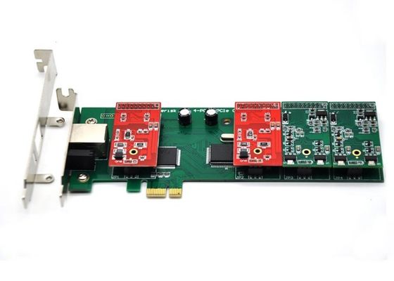
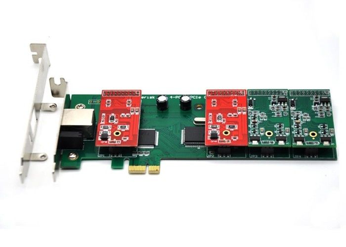
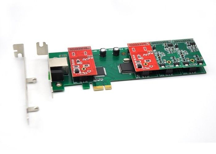
Rohs 94v0 Electronic PCB Printed Circuit Board Assembly Manufacturer OEM PCBA
PCBA Introduction
The English abbreviation of PCBA is Printed Circuit Board Assembly, which means that after PCB blank board is loaded by SMT or DIP plug-in, it is referred to as PCBA. The European and American standard writing is PCB'A, plus "'", this is called the official idiom .
We provide PCB Design & Layout;PCB Prototyping;PCB Fabrication;Turn Prototype PCB Assembly;PCB Assembly Services;PCB'A; BOX assembly,Function Test .
Factory Capacity
| Layers | 1 - 46 L |
| Substrate | FR-4,CTI600,Tg180,,Anti CAF,Halogen-free,,High frequency,Tg170&HF |
| Max. panel size | 700x610mm |
| Board thickness | 0.3 mm - 3.5 mm. |
| Copper thickness | 1/3 oz. to 6 oz. (outer) (Max) |
| Hole | > 0.15mm. |
| Aspect Ratio | 10 : 1 |
| Min. track width | 3.0 mils(partial) |
| Min. track space | 3.0mils(partial) |
| Min. S/M bridge | 3mil |
| Hole plugging diameter | 0.3 mm~0.55 mm. |
| Impedance tolerance | +/- 10%. |
| Color of S/M | green,white,black,red,orange,yellow,blue,purple |
| Surface treatment | OSP,HAL,HAL LF,ENIG,Hard gold,Imm Ag,Imm Sn,Peelable soldermask,Carbon ink print,Selective hard gold |
Our service
![]()
Workshop & Equipment

PCBA Application
Automotive Electronics
Medical Electronics
Smart Home Electronics
Industrial Control
Telecommunications
Security Electronics
![]()
Partners
![]()
Common packaging
PCB: Vacuum packaging with carton box
PCBA: ESD packaging with carton box
![]()
FAQ
1, What service do you provide?
We provide turnkey solution including PCB fabrication, SMT Process, PCB Assembly,final assembly, Function testing and other value-added service.
2, What is needed for PCB & PCBA quotation?
PCB: Quantity, Gerber file and technic requirements(material,size, surface finish treatment, copper thickness,board thickness).
PCBA: PCB information, BOM,Testing documents.
3, How to keep our product information and design file secret ?
We can sign a NDA effect by customers side local law and promising to keep customers data in high confidential level.
4, What are the main products of your PCB/PCBA services?
Automotive, Medical, Industry Control,IOT,Smart Home,Military.
5, What is your minimum order quantity (MOQ)?
Our MOQ is 1 PCS, sample and mass production all can support.
6.What are the services you can provide ?
One-stop contract manufacturing
A:PCB Assembly;
B:PCB Design & Layout
C:PCBA programming & functional testing;
D:Electronic components purchasing service;
E:Enclosure molding & final assembly with labels,instructions,enclosure, boxes.
7.Whether all PCBA s will be tested before delivery ?
Yes , we will test each piece of PCBA product under your testing methods ,to ensure quality and functionality .
8.Do you provide OEM service ?
Yes ,we offer PCB and PCBA OEM Service , we manufacture the PCB and PCBA products to your design and requirements .
9. Do you accept process materials supplied by clients?
A Yes, we can provide component source, and we also accept component from client
Company Information
Haina lean Electronics Co., Ltd is one of the most professional PCB manufacture in Beijing,China.With 8 years of development, Haina Lean Electronics turns into a first class manufacture of HDI PCB ,with production capability 2000 square meters.
Haina Lean Electronics is providing high quality bare PCB,PCB layout design service and PCB assembly service,including components sourcing, function test,conformal coating and complete assembly for clients all.
We have profuse experience in manufacturing PCB,owned experienced technical R & D technology team, young and professional sales and customer service team, experienced and professional procurement team and assembly testing team, which make sure the products quality of the pass rate, on-time delivery rate of customer orders.
Our services include: circuit board design and layout, 2-46 layers PCB manufacturing, professional FPC production, electronic components purchasing, SMT professional processing, Soldering and Assembly, especially sample and small bulk orders. we have the advantages of a quick quote, fast production, fast delivery.
![]()
Our services cover all industries and reach all parts of the world.