-
High Light
enig pcb smt assembly
,military industrial sphere pcb smt assembly
,enig smt board assembly
-
Product Name6L ENIG Military-industrial Sphere PCB Assembly
-
MaterialFr4 High Tg; CEM-1; CEM-3
-
Copper Thickness1/3OZ 1OZ 2OZ ... 6OZ
-
Min. Line Width0.030mm
-
Board ThicknessCore Thickness 0.05mm-1.5mm ,Fineshed Board Thickness 0.3-3.5mm
-
Min. Hole SizeLaser 0.05mm ; Mechnical 0.15
-
Surface FinishingHASL, ENIG, OSP, Lead Free HASL, HASL/OSP/ENIG
-
ServiceODM And OEM PCB PCBA Solutions
-
PCB Assembly MethodMixed; SMT, DIP, THT
-
ApplicationMilitary-Industrial Sphere ,Automotive /automobile , Medical .Communication Solution, Industrial Control, Aerospace , Image Processing ,video Processing Technology ,smart Home ,securit Etc.
-
Place of OriginCHINA
-
Brand NameHNL-PCBA
-
CertificationISO9001,IS16949, ISO14001,ROHS ,UL, IPC-A ,QC080000
-
Model NumberPCB Assembly 04
-
Minimum Order Quantity1 PC
-
PriceNegotiable
-
Packaging DetailsESD packaging with carton box
-
Delivery Time1-7days
-
Payment TermsT/T, Western Union, L/C, MoneyGram
-
Supply Ability10,000,000 Point /Day
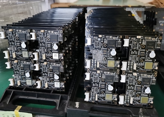
6l Enig Pcb Smt Assembly Military Industrial Sphere


6L ENIG Military-industrial sphere PCB Assembly
Haina Lean is an entity enterprise that specializes in electronic product design and development, supply chain management, PCBA and one-stop (OEM) production services for complete machine products. Also it owns profuse experience in manufacturing PCB,owned experienced technical R & D technology team, young and professional sales and customer service team, experienced and professional procurement team and assembly testing team, which make sure the products quality of the pass rate, on-time delivery rate of customer orders. Welcome to visit our factory!
Our Service
PCB project
PCB design
PCB manufacture
PCB Solutions
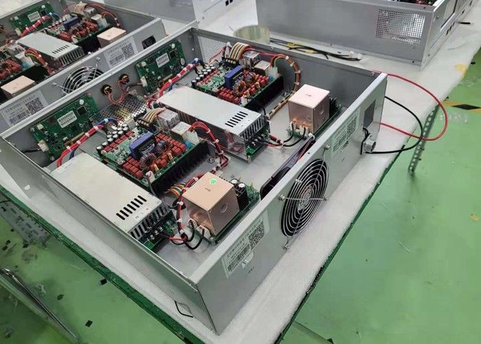
PCB Assembly
Box Assembly
PCB CAPABILITIES
| FACTORY CAPABILITIES | |||
| No. | Items | 2019 | 2020 |
| 1 | HDI Capabilities | HDI ELIC (4+2+4) | HDI ELIC(5+2+5) |
| 2 | Max layer count | 32L | 36L |
| 3 | Board Thickness | Core thickness 0.05mm-1.5mm ,Fineshed board thickness 0.3-3.5mm | Core thickness 0.05mm-1.5mm ,Fineshed board thickness 0.3-3.5mm |
| 4 | Min.Hole Size | Laser 0.075mm | Laser 0.05mm |
| Mechnical 0.15mm | Mechnical 0.15mm | ||
| 5 | Min Line Width/Space | 0.035mm/0.035mm | 0.030mm/0.030mm |
| 6 | Copper Thickness | 1/3oz-4oz | 1/3oz-6oz |
| 7 | Size Max Panel size | 700x610mm | 700x610mm |
| 8 | Registration Accuracy | +/-0.05mm | +/-0.05mm |
| 9 | Routing Accuracy | +/-0.075mm | +/-0.05mm |
| 10 | Min.BGA PAD | 0.15mm | 0.125mm |
| 11 | Max Aspect Ratio | 10:1 | 10:1 |
| 12 | Bow and Twist | 0.50% | 0.50% |
| 13 | Impedance Control Tolerance | +/-8% | +/-5% |
| 14 | Daily Output | 3,000m2 (Max capacity of equipment) | 4,000m2 (Max capacity of equipment) |
| 15 | Surface Finishing | ENEPING /ENIG /HASL /FINGER GOLD/IMMERSION TIN/SELECTIVE THICK GOLD | |
| 16 | Raw Material | FR-4/Normal Tg/High Tg/Low Dk/HF FR4/PTEE/PI | |
| PCBA Capability | |||
| Material Type | Item | Min | Max |
| PCB | Dimension (length,width,height.mm) | 50*40*0.38 | 600*400*4.2 |
| Material | FR-4,CEM-1,CEM-3,Aluminium-based board,Rogers,ceramic plate,FPC | ||
| Surface finish | HASL,OSP,Immersion gold,Flash Gold Finger | ||
| Components | Chip&IC | 1005 | 55mm |
| BGA Pitch | 0.3mm | - | |
| QFP Pitch | 0.3mm | - | |
Our SMT capabilities:
SMT Assembly: SMT provides a flexible high technology. These solutions include:
7 high-speed placement machines,
7 automatic printers with fiducial alignment,
2 X-ray machines,
BGA maintenance machines,
ICT test machines
PCB SMT Assembly Process
1.Solder Paste stenciling---2.Surface Mount Technology (Pick and Place)---3.Reflow Soldering---4.Inspection and Quality Control---5.Through-Hole Component Insertion (DIP Process)---6.Final Inspection and Functional Test
![]()
Our advantage
1.Service value
Independent quotation system to quickly serve the market
2.PCB manufacturing
High-tech PCB and PCB assembly production line
3.Material purchasing
A team of experienced electronic component procurement engineers
4.SMT post soldering
Dust-free workshop, high-end SMT patch processing
![]()
![]()
PCB SMT Assembly Delivery Time
| Product Type | Qty | Normal lead time | Quick-turn lead time |
| SMT+DIP | 1-50 | 1WD-2WD | 8H |
| SMT+DIP | 51-200 | 2WD-3WD | 1.5WD |
| SMT+DIP | 201-2000 | 3WD-4WD | 2WD |
| SMT+DIP | ≥2001 | 4WD-5WD | 3WD |
| PCBA(2-4Layer) | 1-50 | 2.5WD-3.5WD | 1WD |
| PCBA(2-4Layer) | 51-2000 | 5WD-6WD | 2.5WD |
| PCBA(2-4Layer) | ≥2001 | ≥7WD | 5WD |
| PCBA(6-10Layer) | 1-50 | 3WD-4WD | 2.5WD |
| PCBA(6-10Layer) | 51-2000 | 7WD-8WD | 6WD |
| PCBA(10-HDILayer) | 1-50 | 7WD-9WD | 5WD |
| PCBA(10-HDILayer) | 51-2000 | 9WD-11WD | 7WD |
Electronic Board Assembly Application Field
Our products are widely used in Military-Industrial sphere ,Automotive /automobile , Medical .Communication Solution, Industrial Control, Aerospace , image processing ,video processing technology ,smart home ,securit etc.
![]()
Workshop
![]()
![]()
![]()
Common packaging
1.PCB: Vacuum packaging with carton box
2.PCBA: ESD packaging with carton box
![]()
Our services cover all industries and reach all parts of the world.